Note
This page was generated from tut/2-From-components-to-chip/2.24-Design-rule-checking.ipynb.
Design rule checking
A design that renders is not a design that works. Nothing in Quantum Metal stops you from routing a resonator straight through a feedline, from putting a launchpad past the chip edge, or from asking for a 90 um fillet on a 60 um segment. The picture looks plausible; the chip does not.
qiskit_metal.validation is a design rule check (DRC) for that class of mistake. It reads the built qgeometry tables and reports findings:
from qiskit_metal.validation import validate

result = validate(design)
print(result.report())
What the default rules check
Rule |
Catches |
Default |
Source |
|---|---|---|---|
|
two components’ metal overlapping on one layer – a short |
any overlap > 1 um^2 |
– |
|
metal close enough that etch residue can bridge it |
2 um |
GDSII-to-wafer R8 |
|
CPW gap so narrow the interface participation ratio spikes |
3 um |
GDSII-to-wafer R1 |
|
geometry off the die, silently clipped downstream |
– |
– |
|
a segment too short to host its own fillet arc |
fillet radius |
– |
|
a CPW running close enough to a qubit pocket to couple |
3x CPW width |
project heuristic |
|
the ground plane split into disconnected regions |
– |
GDSII-to-wafer R9 |
Severity matters: ERROR is geometry that is wrong regardless of intent, WARNING is legal geometry that is probably unintended or spends a physical budget (loss, stray coupling). Only errors make a result falsy or raise.
These are a starting point, not a foundry sign-off. Every threshold is a constructor argument – see Tuning the rules below.
[1]:
# In Colab / Binder, uncomment to install Quantum Metal (lite, no Qt):
# !pip install -q quantum-metal
[2]:
import qiskit_metal as qm
from qiskit_metal import Dict, designs
from qiskit_metal.qlibrary.qubits.transmon_pocket import TransmonPocket
from qiskit_metal.qlibrary.terminations.launchpad_wb import LaunchpadWirebond
from qiskit_metal.qlibrary.terminations.open_to_ground import OpenToGround
from qiskit_metal.qlibrary.tlines.pathfinder import RoutePathfinder
from qiskit_metal.qlibrary.tlines.straight_path import RouteStraight
from qiskit_metal.validation import validate


def new_design():
    design = designs.DesignPlanar()
    design.overwrite_enabled = True
    design.chips.main.size.size_x = "6mm"
    design.chips.main.size.size_y = "6mm"
    return design


def link(design, name, start, end, ori_start, ori_end, cls=RouteStraight, **options):
    """A CPW between two fresh open terminations -- shorthand for this notebook."""
    OpenToGround(
        design,
        f"{name}_a",
        options=dict(pos_x=start[0], pos_y=start[1], orientation=ori_start),
    )
    OpenToGround(
        design,
        f"{name}_b",
        options=dict(pos_x=end[0], pos_y=end[1], orientation=ori_end),
    )
    return cls(
        design,
        name,
        options=Dict(
            pin_inputs=Dict(
                start_pin=Dict(component=f"{name}_a", pin="open"),
                end_pin=Dict(component=f"{name}_b", pin="open"),
            ),
            **options,
        ),
    )
A design with one defect per rule
Each block below is a mistake that is easy to make and hard to see. Read them now, then look at the plot and try to spot them before running the check.
[3]:
design = new_design()

TransmonPocket(design, "Q1", options=dict(pos_x="0mm", pos_y="0mm"))

# 1. metal-overlap: two CPWs cross. On one layer, that is a short.
link(design, "cross_h", ("-2.6mm", "2mm"), ("-1.2mm", "2mm"), "180", "0")
link(design, "cross_v", ("-1.9mm", "1.4mm"), ("-1.9mm", "2.6mm"), "270", "90")

# 2. metal-spacing: parallel CPWs 1 um apart. Not a short in the CAD, but
#    incomplete etching leaves residue that bridges gaps this narrow.
link(design, "near_a", ("0.6mm", "2.0055mm"), ("2.4mm", "2.0055mm"), "180", "0")
link(design, "near_b", ("0.6mm", "1.9945mm"), ("2.4mm", "1.9945mm"), "180", "0")

# 3. cpw-gap: a 1 um gap concentrates field in the lossy substrate interface.
link(
    design,
    "thin",
    ("-2.6mm", "-2.4mm"),
    ("-0.6mm", "-2.4mm"),
    "180",
    "0",
    trace_gap="1um",
)

# 4. chip-bounds: the launchpad hangs off the die.
LaunchpadWirebond(
    design, "LP", options=dict(pos_x="3.4mm", pos_y="0mm", orientation="180")
)

# 5. short-segment: 100 um legs cannot host a 150 um fillet radius.
link(
    design,
    "kink",
    ("1.2mm", "-2.6mm"),
    ("1.3mm", "-2.5mm"),
    "180",
    "90",
    cls=RoutePathfinder,
    fillet="150um",
)

# 6. qubit-clearance: a CPW skimming Q1's pocket couples to the qubit.
link(design, "hug", ("-1.5mm", "0.35mm"), ("1.5mm", "0.35mm"), "180", "0")

# 7. ground-continuity: a CPW reaching both die edges cuts the ground in two.
link(design, "split", ("-2.994mm", "-1.2mm"), ("2.994mm", "-1.2mm"), "180", "0")

design.rebuild()
design.components.keys()
10:41PM 13s WARNING [check_lengths]: For path table, component=kink, key=trace has short segments that could cause issues with fillet. Values in (1-1)  are index(es) in shapely geometry.
10:41PM 13s WARNING [check_lengths]: For path table, component=kink, key=cut has short segments that could cause issues with fillet. Values in (1-1)  are index(es) in shapely geometry.
10:41PM 13s WARNING [check_lengths]: For path table, component=kink, key=trace has short segments that could cause issues with fillet. Values in (1-1)  are index(es) in shapely geometry.
10:41PM 13s WARNING [check_lengths]: For path table, component=kink, key=cut has short segments that could cause issues with fillet. Values in (1-1)  are index(es) in shapely geometry.
[3]:
['Q1',
 'cross_h_a',
 'cross_h_b',
 'cross_h',
 'cross_v_a',
 'cross_v_b',
 'cross_v',
 'near_a_a',
 'near_a_b',
 'near_a',
 'near_b_a',
 'near_b_b',
 'near_b',
 'thin_a',
 'thin_b',
 'thin',
 'LP',
 'kink_a',
 'kink_b',
 'kink',
 'hug_a',
 'hug_b',
 'hug',
 'split_a',
 'split_b',
 'split']
[4]:
fig = qm.view(design)
qm.show_inline(fig)
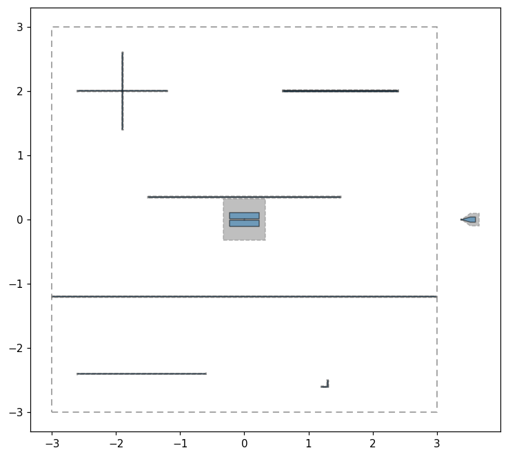
The dashed rectangle is the die outline – qm.view draws it so geometry placed off the chip is visible rather than silently clipped downstream (pass chip_outline=False for the geometry alone). The launchpad on the right is plainly outside it.
The rest are invisible at this zoom. That is the point – the eye checks topology, not micron-scale spacing.
Run the checks
[5]:
result = validate(design)
print(result.report())
10 finding(s) from 11 rule(s): 3 error(s), 7 warning(s)
  [error] metal-overlap: cross_h and cross_v overlap by 100 um^2 of metal on layer 1  @ (-1.9000, 2.0000)
  [error] metal-spacing: near_a and near_b are 1.00 um apart (minimum 2.00 um)  @ (2.4000, 2.0000)
  [warning] cpw-gap: thin has a 1.00 um CPW gap (minimum 3.00 um)  @ (-2.6000, -2.4000)
  [error] chip-bounds: LP extends 660.0 um beyond the 'main' chip outline  @ (3.5175, 0.0000)
  [warning] short-segment: kink.trace segment 0 is 100.0 um long but needs 150.0 um for a 150.0 um fillet  @ (1.2500, -2.6000)
  [warning] short-segment: kink.trace segment 1 is 100.0 um long but needs 150.0 um for a 150.0 um fillet  @ (1.3000, -2.5500)
  [warning] short-segment: kink.cut segment 0 is 100.0 um long but needs 150.0 um for a 150.0 um fillet  @ (1.2500, -2.6000)
  [warning] short-segment: kink.cut segment 1 is 100.0 um long but needs 150.0 um for a 150.0 um fillet  @ (1.3000, -2.5500)
  [warning] qubit-clearance: hug passes 14.0 um from Q1's pocket (0.64x CPW width; want 3.0x = 66 um)  @ (0.0000, 0.3500)
  [warning] ground-continuity: ground plane on layer 1 is split into 2 disconnected regions (mm^2: 24.528, 10.705); confirm airbridges or vias tie them together -- this check sees only same-layer metal  @ (0.0000, -1.8000)
Reading the result
validate returns a ValidationResult. It is falsy when there are errors, so it drops straight into an if. Each Finding is a frozen dataclass with the rule name, severity, message, the components involved, an (x, y) location in millimetres, and the measured value against the limit it missed.
[6]:
print("passes:", bool(result))
print("errors:", len(result.errors), " warnings:", len(result.warnings))

worst = result.errors[0]
print()
print("rule:      ", worst.rule)
print("severity:  ", worst.severity)
print("components:", worst.components)
print("location:  ", worst.location)
print("value/limit:", worst.value, "/", worst.limit)
passes: False
errors: 3  warnings: 7

rule:       metal-overlap
severity:   error
components: ('cross_h', 'cross_v')
location:   (-1.9, 2.0)
value/limit: 9.999999999999574e-05 / 1e-06
[7]:
# Group by rule to see the shape of the problem rather than a flat list.
from collections import Counter

Counter(f.rule for f in result.findings)
[7]:
Counter({'short-segment': 4,
         'metal-overlap': 1,
         'metal-spacing': 1,
         'cpw-gap': 1,
         'chip-bounds': 1,
         'qubit-clearance': 1,
         'ground-continuity': 1})
Fixing them
Each finding names the physics it protects, so the fix is not arbitrary.
``metal-overlap`` – move
cross_vclear ofcross_h. If the crossing is deliberate, carry one line over the other on an airbridge. Drawing a bridge on top is not enough: the two lines still overlap on the base layer. See Deliberate crossings below.``metal-spacing`` – open the gap to 200 um. The 2 um default comes from published superconducting-chip rule sets; your foundry sets the real number.
``cpw-gap`` – back to the standard 6 um. Narrow gaps push field into the substrate-metal interface, where two-level-system loss lives.
``chip-bounds`` – pull the launchpad onto the die, or grow the die. Off-chip geometry is silently clipped by the GDS and FEM renderers.
``short-segment`` – either lengthen the legs or shrink the fillet. A segment must be at least the fillet radius long (twice, if it is an interior segment with a corner at each end) or the renderer drops the arc and you get a sharp corner – a current crowding point.
``qubit-clearance`` – move the CPW away from the pocket. This is a project heuristic, not a literature value: 3x the CPW width is a conservative starting point, not a coupling calculation.
``ground-continuity`` – stop the CPW short of the die edges so ground can flow around it. A split ground plane is not automatically wrong – airbridges tie the pieces together and this rule cannot see them – but an unintended split hosts slotline modes.
[8]:
design = new_design()

TransmonPocket(design, "Q1", options=dict(pos_x="0mm", pos_y="0mm"))

link(design, "cross_h", ("-2.6mm", "2mm"), ("-1.2mm", "2mm"), "180", "0")
link(design, "cross_v", ("-1.9mm", "1.2mm"), ("-1.9mm", "1.7mm"), "270", "90")
link(design, "near_a", ("0.6mm", "2.1mm"), ("2.4mm", "2.1mm"), "180", "0")
link(design, "near_b", ("0.6mm", "1.9mm"), ("2.4mm", "1.9mm"), "180", "0")
link(
    design,
    "thin",
    ("-2.6mm", "-2.4mm"),
    ("-0.6mm", "-2.4mm"),
    "180",
    "0",
    trace_gap="6um",
)
LaunchpadWirebond(
    design, "LP", options=dict(pos_x="2.5mm", pos_y="0mm", orientation="180")
)
link(
    design,
    "kink",
    ("0.9mm", "-2.6mm"),
    ("1.6mm", "-2.0mm"),
    "180",
    "90",
    cls=RoutePathfinder,
    fillet="90um",
)
link(design, "hug", ("-1.5mm", "0.7mm"), ("1.5mm", "0.7mm"), "180", "0")
link(design, "split", ("-2.4mm", "-1.2mm"), ("2.4mm", "-1.2mm"), "180", "0")

design.rebuild()

result = validate(design)
print(result.report())
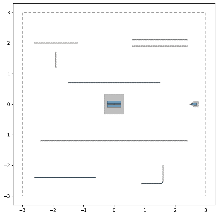
Design rules passed (11 rules ran, no findings).
[9]:
fig = qm.view(design)
qm.show_inline(fig)
Deliberate crossings
The rules check metal on each layer. An Airbridge puts its span and landing pads on their own layers (30 and 31 by default), so placing one over the crossing changes nothing on layer 1: the two lines still overlap, and the check still reports a short.
[10]:
from qiskit_metal.qlibrary.tlines.airbridge import Airbridge
from qiskit_metal.validation import Waiver

crossing = new_design()
link(crossing, "cross_h", ("-2.6mm", "2mm"), ("-1.2mm", "2mm"), "180", "0")
link(crossing, "cross_v", ("-1.9mm", "1.4mm"), ("-1.9mm", "2.6mm"), "270", "90")
Airbridge(
    crossing, "AB", options=dict(pos_x="-1.9mm", pos_y="2mm", crossover_length="30um")
)
crossing.rebuild()

print(validate(crossing).report())
1 finding(s) from 11 rule(s): 1 error(s), 0 warning(s)
  [error] metal-overlap: cross_h and cross_v overlap by 100 um^2 of metal on layer 1  @ (-1.9000, 2.0000)
For a real crossover, cut the upper line where it crosses and connect the two cut ends to the bridge’s pins a and b. The line is then continuous through the bridge, nothing overlaps on layer 1, and the check passes.
[11]:
crossing = new_design()
link(crossing, "cross_v", ("-1.9mm", "1.4mm"), ("-1.9mm", "2.6mm"), "270", "90")
OpenToGround(
    crossing, "h_west", options=dict(pos_x="-2.6mm", pos_y="2mm", orientation="180")
)
OpenToGround(
    crossing, "h_east", options=dict(pos_x="-1.2mm", pos_y="2mm", orientation="0")
)
Airbridge(
    crossing, "AB", options=dict(pos_x="-1.9mm", pos_y="2mm", crossover_length="30um")
)

# cross_h, cut in two at the bridge: west end -> pin a, pin b -> east end.
for name, start, end in [
    ("cross_h_west", ("h_west", "open"), ("AB", "a")),
    ("cross_h_east", ("AB", "b"), ("h_east", "open")),
]:
    RouteStraight(
        crossing,
        name,
        options=Dict(
            pin_inputs=Dict(
                start_pin=Dict(component=start[0], pin=start[1]),
                end_pin=Dict(component=end[0], pin=end[1]),
            )
        ),
    )
crossing.rebuild()

print(validate(crossing).report())
Design rules passed (11 rules ran, no findings).
If the layout keeps the lines whole on purpose – for example, the crossovers are cut and bridged later in the mask flow – keep the crossing and record a Waiver instead. A waiver needs a reason, can be limited to one rule, the components involved and a maximum value, and does not hide anything: the waived finding is still listed in the report, it just no longer counts as an error. Do not widen the rule’s threshold instead; that would also hide real shorts.
[12]:
crossing = new_design()
link(crossing, "cross_h", ("-2.6mm", "2mm"), ("-1.2mm", "2mm"), "180", "0")
link(crossing, "cross_v", ("-1.9mm", "1.4mm"), ("-1.9mm", "2.6mm"), "270", "90")
crossing.rebuild()

waiver = Waiver(
    "cross_v is carried over cross_h on an airbridge in the mask flow",
    rule="metal-overlap",
    components=("cross_h", "cross_v"),
    max_value=200e-6,  # mm^2: this crossing overlaps by 100 um^2
)
result = validate(crossing, waivers=[waiver])
print("passes:", bool(result))
print(result.report())
passes: True
Design rules passed (11 rules ran, no findings).
1 waived:
  [error] metal-overlap: cross_h and cross_v overlap by 100 um^2 of metal on layer 1  @ (-1.9000, 2.0000)
      waived: cross_v is carried over cross_h on an airbridge in the mask flow
Tuning the rules
Thresholds are constructor arguments, so a process design kit that differs from the defaults is a call, not a fork. Pass rules= to run a different set – either a subset, or the defaults with one swapped out.
[13]:
from qiskit_metal.validation import DEFAULT_RULES, CPWGapRule, MetalSpacingRule

# Just one rule, at a tighter limit than the default.
print(validate(design, rules=[CPWGapRule(min_gap="10um")]).report())
8 finding(s) from 1 rule(s): 0 error(s), 8 warning(s)
  [warning] cpw-gap: cross_h has a 6.00 um CPW gap (minimum 10.00 um)  @ (-1.2000, 2.0000)
  [warning] cpw-gap: cross_v has a 6.00 um CPW gap (minimum 10.00 um)  @ (-1.9000, 1.2000)
  [warning] cpw-gap: near_a has a 6.00 um CPW gap (minimum 10.00 um)  @ (2.4000, 2.1000)
  [warning] cpw-gap: near_b has a 6.00 um CPW gap (minimum 10.00 um)  @ (2.4000, 1.9000)
  [warning] cpw-gap: thin has a 6.00 um CPW gap (minimum 10.00 um)  @ (-2.6000, -2.4000)
  [warning] cpw-gap: kink has a 6.00 um CPW gap (minimum 10.00 um)  @ (1.6000, -2.6000)
  [warning] cpw-gap: hug has a 6.00 um CPW gap (minimum 10.00 um)  @ (-1.5000, 0.7000)
  [warning] cpw-gap: split has a 6.00 um CPW gap (minimum 10.00 um)  @ (-2.4000, -1.2000)
[14]:
# The 2 um default is a fabrication limit. A crosstalk budget is a separate,
# much looser constraint -- unconnected CPWs kept 250 um apart. Replacing the
# rule rather than adding one matters: both copies would run, and the design
# would be reported twice.
house_rules = [r for r in DEFAULT_RULES if r.name != "metal-spacing"]
house_rules.append(MetalSpacingRule(min_spacing="250um"))

print(validate(design, rules=house_rules).report())
1 finding(s) from 11 rule(s): 1 error(s), 0 warning(s)
  [error] metal-spacing: near_a and near_b are 190.00 um apart (minimum 250.00 um)  @ (2.4000, 2.0000)
Severity is an argument too. Promote a warning to an error when your process treats it as a hard rule, and the result turns falsy.
[15]:
from qiskit_metal.validation import Severity

strict_gap = CPWGapRule(min_gap="10um", severity=Severity.ERROR)
print(bool(validate(design, rules=[strict_gap])))
False
Failing the build
In a design script or CI job you want the check to stop the run, not print. strict=True raises DesignRuleViolation on any error.
[16]:
from qiskit_metal.validation import DesignRuleViolation

try:
    validate(design, rules=[strict_gap], strict=True)
except DesignRuleViolation as exc:
    print("build stopped:")
    print(str(exc).splitlines()[0])
build stopped:
8 finding(s) from 1 rule(s): 8 error(s), 0 warning(s)
The same thing, without exceptions, at the end of a build script:
result = validate(design)
if not result:
    print(result.report())
    raise SystemExit(1)
Quantum Metal gates its own shipped reference designs this way – see tests/test_reference_designs.py.
Writing your own rule
A rule is any object with a name, a description, and a check(design) that yields Findings. Subclass DesignRule and use the same helpers the built-in rules use: chip_bounds, component_geometry (which unions each component’s drawn metal, per layer if you ask), and representative_point.
Here is a fab rule the defaults do not cover: nothing may reach into the dicing street at the die edge.
[17]:
from shapely.geometry import box

from qiskit_metal.validation import (
    DesignRule,
    Finding,
    chip_bounds,
    component_geometry,
    representative_point,
)


class KeepOutBorderRule(DesignRule):
    """Metal must stay clear of the dicing street at the chip edge."""

    name = "keep-out-border"
    description = "Metal reaches into the dicing street."

    def __init__(self, margin="400um", severity=Severity.ERROR):
        self.margin = margin
        self.severity = severity

    def check(self, design):
        margin = design.parse_value(self.margin)
        minx, miny, maxx, maxy = chip_bounds(design)
        keep_in = box(minx + margin, miny + margin, maxx - margin, maxy - margin)

        for name, geometry in component_geometry(design).items():
            outside = geometry.difference(keep_in)
            if outside.is_empty:
                continue
            yield Finding(
                rule=self.name,
                severity=self.severity,
                message=(
                    f"{name} reaches {margin * 1000:.0f} um into the dicing street"
                ),
                components=(name,),
                location=representative_point(outside),
                value=outside.area,
                limit=0.0,
            )


print(validate(design, rules=[KeepOutBorderRule()]).report())
2 finding(s) from 1 rule(s): 2 error(s), 0 warning(s)
  [error] keep-out-border: kink reaches 400 um into the dicing street  @ (1.2521, -2.6026)
  [error] keep-out-border: LP reaches 400 um into the dicing street  @ (2.6510, 0.0000)
What this does not check
DRC is a geometry check. It says nothing about whether your resonator is at the frequency you wanted, whether the coupling is right, or whether the qubit is anharmonic enough – those need the analysis notebooks in section 4. It also knows nothing about your foundry’s actual rule deck; the defaults are a published starting point.
Three known limits worth stating plainly:
Layers are trusted. Overlap and spacing are checked per layer, so metal on layer 30 crossing metal on layer 1 is fine. If your stack does not match that assumption, the rules will miss real shorts.
``net_info`` is trusted. Components joined through a pin are exempt from the overlap and spacing rules, because a route abutting its termination is not a short.
``ground-continuity`` sees one layer. It reports that the ground is split, not that a piece is floating – an airbridge on another layer may well tie the pieces together.
References
From GDSII to Wafer: EDA Design Flow and Data Conversion for Wafer-Scale Manufacturing of Superconducting Quantum Chips, arXiv:2604.11379 – the R1 / R8 / R9 thresholds used above.
A Review of Design Concerns in Superconducting Quantum Circuits, arXiv:2411.16967 – crosstalk mechanisms and airbridge placement.
Airbridges in Quantum Metal: tutorial 2.15.
Full worked designs that pass these rules: Appendix A.
For more information, review the Introduction to Quantum Computing and Quantum Hardware lectures below
|
Lecture Video | Lecture Notes | Lab |
|
Lecture Video | Lecture Notes | Lab |
|
Lecture Video | Lecture Notes | Lab |
|
Lecture Video | Lecture Notes | Lab |
|
Lecture Video | Lecture Notes | Lab |
|
Lecture Video | Lecture Notes | Lab |