Note
This page was generated from tut/1-Overview/1.3-Saving-Your-Chip-Design.ipynb.
1.3 Saving Your Chip Design
By the end of this tutorial you will know how to:
Export a design to a Python script (
to_python_script) — the reproducibility superpowerExport to GDS for fabrication, and visually inspect the result
We start from the full 2-qubit chip built in tutorial 1.2. The block below is exactly what design.to_python_script() produces — a self-contained Python definition you can version-control, share, and replay.
[ ]:
# === Design reproduced from tutorial 1.2 via design.to_python_script() ===
from qiskit_metal import designs, Dict
from qiskit_metal.qlibrary.qubits.transmon_pocket_cl import TransmonPocketCL
from qiskit_metal.qlibrary.tlines.pathfinder import RoutePathfinder
from qiskit_metal.qlibrary.tlines.meandered import RouteMeander
from qiskit_metal.qlibrary.lumped.cap_3_interdigital import Cap3Interdigital
from qiskit_metal.qlibrary.terminations.launchpad_wb import LaunchpadWirebond

design = designs.DesignPlanar()
design.overwrite_enabled = True

Q1 = TransmonPocketCL(
    design,
    "Q1",
    options=dict(
        pos_x="0.7mm",
        pos_y="0mm",
        orientation="0",
        pad_gap="30um",
        inductor_width="20um",
        pad_width="425 um",
        pad_height="90um",
        pocket_width="650um",
        pocket_height="650um",
        gds_cell_name="FakeJunction_01",
        make_CL=True,
        cl_gap="6um",
        cl_width="10um",
        cl_length="20um",
        cl_ground_gap="6um",
        cl_pocket_edge="180",
        cl_off_center="50um",
        connection_pads=dict(
            readout=dict(
                loc_W=1,
                loc_H=1,
                pad_gap="15um",
                pad_width="125um",
                pad_height="30um",
                cpw_extend="100um",
                pocket_extent="5um",
                pocket_rise="65um",
            ),
            bus=dict(
                loc_W=-1,
                loc_H=-1,
                pad_gap="15um",
                pad_width="125um",
                pad_height="30um",
                cpw_extend="100um",
                pocket_extent="5um",
                pocket_rise="65um",
            ),
        ),
    ),
    make=True,
)

Q2 = TransmonPocketCL(
    design,
    "Q2",
    options=dict(
        pos_x="-0.7mm",
        pos_y="0mm",
        orientation="180",
        pad_gap="30um",
        inductor_width="20um",
        pad_width="425 um",
        pad_height="90um",
        pocket_width="650um",
        pocket_height="650um",
        gds_cell_name="FakeJunction_01",
        make_CL=True,
        cl_gap="6um",
        cl_width="10um",
        cl_length="20um",
        cl_ground_gap="6um",
        cl_pocket_edge="180",
        cl_off_center="50um",
        connection_pads=dict(
            readout=dict(
                loc_W=1,
                loc_H=1,
                pad_gap="15um",
                pad_width="125um",
                pad_height="30um",
                cpw_extend="100um",
                pocket_extent="5um",
                pocket_rise="65um",
            ),
            bus=dict(
                loc_W=-1,
                loc_H=-1,
                pad_gap="15um",
                pad_width="125um",
                pad_height="30um",
                cpw_extend="100um",
                pocket_extent="5um",
                pocket_rise="65um",
            ),
        ),
    ),
    make=True,
)

Bus_Q1_Q2 = RoutePathfinder(
    design,
    "Bus_Q1_Q2",
    options=dict(
        pin_inputs=dict(
            start_pin=dict(component="Q1", pin="bus"),
            end_pin=dict(component="Q2", pin="bus"),
        ),
        fillet="99um",
        total_length="7mm",
        layer="1",
        lead=dict(start_straight="0mm", end_straight="250um"),
        advanced=dict(avoid_collision="true"),
        step_size="0.25mm",
    ),
)

Cap_Q1 = Cap3Interdigital(
    design,
    "Cap_Q1",
    options=dict(
        layer="1",
        pos_x="2.5mm",
        pos_y="0.25mm",
        orientation="90",
        trace_width="10um",
        finger_length="40um",
    ),
)
Cap_Q2 = Cap3Interdigital(
    design,
    "Cap_Q2",
    options=dict(
        layer="1",
        pos_x="-2.5mm",
        pos_y="-0.25mm",
        orientation="-90",
        trace_width="10um",
        finger_length="40um",
    ),
)

Readout_Q1 = RouteMeander(
    design,
    "Readout_Q1",
    options=dict(
        pin_inputs=dict(
            start_pin=dict(component="Q1", pin="readout"),
            end_pin=dict(component="Cap_Q1", pin="a"),
        ),
        fillet="99um",
        total_length="5mm",
        layer="1",
        lead=dict(start_straight="0.325mm", end_straight="125um"),
        meander=dict(spacing="200um", asymmetry="-50um"),
    ),
)
Readout_Q2 = RouteMeander(
    design,
    "Readout_Q2",
    options=dict(
        pin_inputs=dict(
            start_pin=dict(component="Q2", pin="readout"),
            end_pin=dict(component="Cap_Q2", pin="a"),
        ),
        fillet="99um",
        total_length="6mm",
        layer="1",
        lead=dict(start_straight="0.325mm", end_straight="125um"),
        meander=dict(spacing="200um", asymmetry="-50um"),
    ),
)

for name, px, py, ori in [
    ("Launch_Q1_Read", "3.5mm", "0um", "180"),
    ("Launch_Q2_Read", "-3.5mm", "0um", "0"),
    ("Launch_Q1_CL", "1.35mm", "-2.5mm", "90"),
    ("Launch_Q2_CL", "-1.35mm", "2.5mm", "-90"),
]:
    LaunchpadWirebond(
        design,
        name,
        options=dict(
            layer="1",
            pos_x=px,
            pos_y=py,
            orientation=ori,
            trace_width="cpw_width",
            trace_gap="cpw_gap",
            lead_length="25um",
        ),
    )

for name, src_comp, src_pin, dst_comp, dst_pin, length in [
    ("TL_Q1", "Launch_Q1_Read", "tie", "Cap_Q1", "b", "7mm"),
    ("TL_Q2", "Launch_Q2_Read", "tie", "Cap_Q2", "b", "7mm"),
    ("TL_Q1_CL", "Launch_Q1_CL", "tie", "Q1", "Charge_Line", "7mm"),
    ("TL_Q2_CL", "Launch_Q2_CL", "tie", "Q2", "Charge_Line", "7mm"),
]:
    RoutePathfinder(
        design,
        name,
        options=dict(
            pin_inputs=dict(
                start_pin=dict(component=src_comp, pin=src_pin),
                end_pin=dict(component=dst_comp, pin=dst_pin),
            ),
            fillet="99um",
            total_length=length,
            layer="1",
            lead=dict(start_straight="0mm", end_straight="150um"),
            advanced=dict(avoid_collision="true"),
            step_size="0.25mm",
        ),
    )

print(f"Design ready: {len(design.components)} components")
Design ready: 15 components
[ ]:
%matplotlib inline
import matplotlib.pyplot as plt
import qiskit_metal as qm
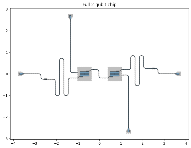
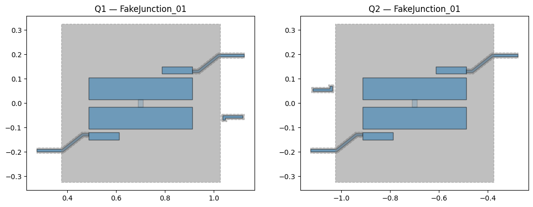
fig_full = qm.view(design, figsize=(9, 9), title="Full 2-qubit chip")
fig, axes = plt.subplots(1, 2, figsize=(13, 6))
qm.view(design, components=["Q1"], title="Q1 — FakeJunction_01", ax=axes[0])
qm.view(design, components=["Q2"], title="Q2 — FakeJunction_01", ax=axes[1])
plt.tight_layout()
plt.close(fig)
display(fig_full)
display(fig)
<Figure size 640x480 with 0 Axes>
[5]:
design.to_python_script()
[5]:
"\nfrom qiskit_metal.qlibrary.lumped.cap_3_interdigital import Cap3Interdigital\n\nfrom qiskit_metal.qlibrary.terminations.launchpad_wb import LaunchpadWirebond\n\nfrom qiskit_metal.qlibrary.tlines.pathfinder import RoutePathfinder\n\nfrom qiskit_metal.qlibrary.tlines.meandered import RouteMeander\n\nfrom qiskit_metal.qlibrary.qubits.transmon_pocket_cl import TransmonPocketCL\n\nfrom qiskit_metal import designs, MetalGUI\n\ndesign = designs.DesignPlanar()\n\ngui = MetalGUI(design)\n\n\n\n # WARNING\n#options_connection_pads failed to have a value\nQ1 = TransmonPocketCL(\ndesign,\nname='Q1',\noptions={'cl_pocket_edge': '180',\n 'connection_pads': {'bus': {'cpw_extend': '100um',\n 'cpw_gap': 'cpw_gap',\n 'cpw_width': 'cpw_width',\n 'loc_H': -1,\n 'loc_W': -1,\n 'pad_cpw_extent': '25um',\n 'pad_cpw_shift': '5um',\n 'pad_gap': '15um',\n 'pad_height': '30um',\n 'pad_width': '125um',\n 'pocket_extent': '5um',\n 'pocket_rise': '65um'},\n 'readout': {'cpw_extend': '100um',\n 'cpw_gap': 'cpw_gap',\n 'cpw_width': 'cpw_width',\n 'loc_H': 1,\n 'loc_W': 1,\n 'pad_cpw_extent': '25um',\n 'pad_cpw_shift': '5um',\n 'pad_gap': '15um',\n 'pad_height': '30um',\n 'pad_width': '125um',\n 'pocket_extent': '5um',\n 'pocket_rise': '65um'}},\n 'gds_cell_name': 'FakeJunction_01',\n 'hfss_inductance': '14nH',\n 'orientation': '0',\n 'pad_width': '425 um',\n 'pos_x': '0.7mm',\n 'pos_y': '0mm'}\n)\n\n\n\n\n\n # WARNING\n#options_connection_pads failed to have a value\nQ2 = TransmonPocketCL(\ndesign,\nname='Q2',\noptions={'cl_pocket_edge': '180',\n 'connection_pads': {'bus': {'cpw_extend': '100um',\n 'cpw_gap': 'cpw_gap',\n 'cpw_width': 'cpw_width',\n 'loc_H': -1,\n 'loc_W': -1,\n 'pad_cpw_extent': '25um',\n 'pad_cpw_shift': '5um',\n 'pad_gap': '15um',\n 'pad_height': '30um',\n 'pad_width': '125um',\n 'pocket_extent': '5um',\n 'pocket_rise': '65um'},\n 'readout': {'cpw_extend': '100um',\n 'cpw_gap': 'cpw_gap',\n 'cpw_width': 'cpw_width',\n 'loc_H': 1,\n 'loc_W': 1,\n 'pad_cpw_extent': '25um',\n 'pad_cpw_shift': '5um',\n 'pad_gap': '15um',\n 'pad_height': '30um',\n 'pad_width': '125um',\n 'pocket_extent': '5um',\n 'pocket_rise': '65um'}},\n 'gds_cell_name': 'FakeJunction_02',\n 'hfss_inductance': '12nH',\n 'orientation': '180',\n 'pad_width': '425 um',\n 'pos_x': '-0.7mm',\n 'pos_y': '0mm'}\n)\n\n\n\n\nBus_Q1_Q2 = RoutePathfinder(\ndesign,\nname='Bus_Q1_Q2',\noptions={'_actual_length': '0.8550176727053895 '\n 'mm',\n 'fillet': '99um',\n 'lead': {'end_jogged_extension': '',\n 'end_straight': '250um',\n 'start_jogged_extension': '',\n 'start_straight': '0mm'},\n 'pin_inputs': {'end_pin': {'component': 'Q2',\n 'pin': 'bus'},\n 'start_pin': {'component': 'Q1',\n 'pin': 'bus'}},\n 'trace_gap': 'cpw_gap'},\n\ntype='CPW',\n)\n\n\n\n\nCap_Q1 = Cap3Interdigital(\ndesign,\nname='Cap_Q1',\noptions={'finger_length': '40um',\n 'orientation': '90',\n 'pos_x': '2.5mm',\n 'pos_y': '0.25mm'},\n\ncomponent_template=None,\n)\n\n\n\n\nCap_Q2 = Cap3Interdigital(\ndesign,\nname='Cap_Q2',\noptions={'finger_length': '40um',\n 'orientation': '-90',\n 'pos_x': '-2.5mm',\n 'pos_y': '-0.25mm'},\n\ncomponent_template=None,\n)\n\n\n\n\nReadout_Q1 = RouteMeander(\ndesign,\nname='Readout_Q1',\noptions={'_actual_length': '5.000000000000001 '\n 'mm',\n 'fillet': '99um',\n 'lead': {'end_jogged_extension': '',\n 'end_straight': '125um',\n 'start_jogged_extension': '',\n 'start_straight': '0.325mm'},\n 'meander': {'asymmetry': '-50um',\n 'spacing': '200um'},\n 'pin_inputs': {'end_pin': {'component': 'Cap_Q1',\n 'pin': 'a'},\n 'start_pin': {'component': 'Q1',\n 'pin': 'readout'}},\n 'total_length': '5mm',\n 'trace_gap': 'cpw_gap'},\n\ntype='CPW',\n)\n\n\n\n\nReadout_Q2 = RouteMeander(\ndesign,\nname='Readout_Q2',\noptions={'_actual_length': '5.999999999999999 '\n 'mm',\n 'fillet': '99um',\n 'lead': {'end_jogged_extension': '',\n 'end_straight': '125um',\n 'start_jogged_extension': '',\n 'start_straight': '0.325mm'},\n 'meander': {'asymmetry': '-50um',\n 'spacing': '200um'},\n 'pin_inputs': {'end_pin': {'component': 'Cap_Q2',\n 'pin': 'a'},\n 'start_pin': {'component': 'Q2',\n 'pin': 'readout'}},\n 'total_length': '6mm',\n 'trace_gap': 'cpw_gap'},\n\ntype='CPW',\n)\n\n\n\n\nLaunch_Q1_Read = LaunchpadWirebond(\ndesign,\nname='Launch_Q1_Read',\noptions={'orientation': '180',\n 'pos_x': '3.5mm',\n 'pos_y': '0um'},\n\ncomponent_template=None,\n)\n\n\n\n\nLaunch_Q2_Read = LaunchpadWirebond(\ndesign,\nname='Launch_Q2_Read',\noptions={'orientation': '0',\n 'pos_x': '-3.5mm',\n 'pos_y': '0um'},\n\ncomponent_template=None,\n)\n\n\n\n\nLaunch_Q1_CL = LaunchpadWirebond(\ndesign,\nname='Launch_Q1_CL',\noptions={'orientation': '90',\n 'pos_x': '1.35mm',\n 'pos_y': '-2.5mm'},\n\ncomponent_template=None,\n)\n\n\n\n\nLaunch_Q2_CL = LaunchpadWirebond(\ndesign,\nname='Launch_Q2_CL',\noptions={'orientation': '-90',\n 'pos_x': '-1.35mm',\n 'pos_y': '2.5mm'},\n\ncomponent_template=None,\n)\n\n\n\n\nTL_Q1 = RoutePathfinder(\ndesign,\nname='TL_Q1',\noptions={'_actual_length': '1.0750176727053897 '\n 'mm',\n 'fillet': '99um',\n 'lead': {'end_jogged_extension': '',\n 'end_straight': '150um',\n 'start_jogged_extension': '',\n 'start_straight': '0mm'},\n 'pin_inputs': {'end_pin': {'component': 'Cap_Q1',\n 'pin': 'b'},\n 'start_pin': {'component': 'Launch_Q1_Read',\n 'pin': 'tie'}},\n 'trace_gap': 'cpw_gap'},\n\ntype='CPW',\n)\n\n\n\n\nTL_Q2 = RoutePathfinder(\ndesign,\nname='TL_Q2',\noptions={'_actual_length': '1.0750176727053897 '\n 'mm',\n 'fillet': '99um',\n 'lead': {'end_jogged_extension': '',\n 'end_straight': '150um',\n 'start_jogged_extension': '',\n 'start_straight': '0mm'},\n 'pin_inputs': {'end_pin': {'component': 'Cap_Q2',\n 'pin': 'b'},\n 'start_pin': {'component': 'Launch_Q2_Read',\n 'pin': 'tie'}},\n 'trace_gap': 'cpw_gap'},\n\ntype='CPW',\n)\n\n\n\n\nTL_Q1_CL = RoutePathfinder(\ndesign,\nname='TL_Q1_CL',\noptions={'_actual_length': '2.610508836352695 '\n 'mm',\n 'fillet': '99um',\n 'lead': {'end_jogged_extension': '',\n 'end_straight': '150um',\n 'start_jogged_extension': '',\n 'start_straight': '0mm'},\n 'pin_inputs': {'end_pin': {'component': 'Q1',\n 'pin': 'Charge_Line'},\n 'start_pin': {'component': 'Launch_Q1_CL',\n 'pin': 'tie'}},\n 'trace_gap': 'cpw_gap'},\n\ntype='CPW',\n)\n\n\n\n\nTL_Q2_CL = RoutePathfinder(\ndesign,\nname='TL_Q2_CL',\noptions={'_actual_length': '2.610508836352695 '\n 'mm',\n 'fillet': '99um',\n 'lead': {'end_jogged_extension': '',\n 'end_straight': '150um',\n 'start_jogged_extension': '',\n 'start_straight': '0mm'},\n 'pin_inputs': {'end_pin': {'component': 'Q2',\n 'pin': 'Charge_Line'},\n 'start_pin': {'component': 'Launch_Q2_CL',\n 'pin': 'tie'}},\n 'trace_gap': 'cpw_gap'},\n\ntype='CPW',\n)\n\n\n\ngui.rebuild()\ngui.autoscale()\n "
Saving with to_python_script()
design.to_python_script() serialises the entire design state — every component, every option, every route — into a self-contained Python script. Running that script recreates the design identically, with no dependency on the original notebook session.
When to use it:
Version control — commit the
.pyfile alongside your notebook; diffs are readableSharing — send the script to a collaborator who can reproduce the exact design
Headless / batch — run the script in CI or a parameter sweep without launching the GUI
Long-term archiving — the script is plain Python, readable years later without notebook tooling
The output prints to the cell below. Copy it into the cell underneath and run it to verify it reproduces your design cleanly.
Replay the saved script
Copy the output from the cell above into a fresh code cell (or a .py file) and run it. It should rebuild the full design without any of the intermediate cells above.
You can also save it directly to a file:
import pathlib

script = design.to_python_script()          # returns the script as a string
pathlib.Path("my_chip_design.py").write_text(script)
print("Saved to my_chip_design.py")
Then replay from the command line:
python my_chip_design.py
Tip: the script is deterministic — running it twice produces the same geometry. This makes it safe to use as a fixture in automated tests or as input to a parameter sweep.
Exporting to GDS
to_python_script() captures your design intent; GDS export produces the fabrication mask. The GDS renderer handles junction placement, ground-plane cheesing, and layer assignment.
gds = design.renderers.gds

# Point to a GDS file containing your Josephson junction cells.
# The file can use any unit (µm, nm, mm) — the renderer auto-scales.
gds.options.path_filename = "../resources/Fake_Junctions.GDS"

# Control whether cheese/no-cheese geometry appears in the output.
# {1: False} = process layer 1 but suppress cheese holes from the file.
# Using Dict(main={}) omits the layer entirely and triggers a warning.
gds.options.cheese.view_in_file    = Dict(main={1: False})
gds.options.no_cheese.view_in_file = Dict(main={1: False})

gds.export_to_gds("my_chip.gds")
After export, inspect the result:
import gdstk

lib = gdstk.read_gds("my_chip.gds")

# show=True embeds an SVG preview directly in this cell output.
# Increase scale for a larger chip; increase width to fill the cell.
gds.debug_summarize_gds_library(lib, show=True, scale=100, width=900)
Junction units
The qubit components in this design use gds_cell_name to name the junction placeholder:
Qubit |
|
|---|---|
Q1 |
|
Q2 |
|
These names must match cells inside the GDS file pointed to by path_filename. The renderer reads the file’s unit field and rescales all junction geometry automatically — a junction file in nm, µm, or any other unit will land at the correct physical size. See 1.2 Quick start → Render to GDS for a full walkthrough including layer options and the debug summary tool.
What’s next
1.4 Headless quick view — run and visualise this design without the Qt GUI
2 From components to chip — multi-qubit designs, CPW routing, and design variables
3 Renderers — HFSS, Q3D, GDS, and gmsh/Elmer in depth
[12]:
from qiskit_metal import MetalGUI, Dict, open_docs

gds = design.renderers.gds

# Point to a GDS file containing your Josephson junction cells.
# The file can use any unit (µm, nm, mm) — the renderer auto-scales.
gds.options.path_filename = "../resources/Fake_Junctions.GDS"

# Control whether cheese/no-cheese geometry appears in the output.
# {1: False} = process layer 1 but suppress cheese holes from the file.
# Using Dict(main={}) omits the layer entirely and triggers a warning.
gds.options.cheese.view_in_file = Dict(main={1: False})
gds.options.no_cheese.view_in_file = Dict(main={1: False})

gds.export_to_gds("my_chip.gds")
10:21PM 29s INFO [import_junction_gds_file]: Rescaling imported junction library from unit=1e-06 to unit=0.001 (scale factor=0.001).
[12]:
1
[15]:
import gdstk

lib = gdstk.read_gds("my_chip.gds")

# show=True embeds an SVG preview directly in this cell output.
# Increase scale for a larger chip; increase width to fill the cell.
gds.debug_summarize_gds_library(lib, show=True, scale=100, width=900)
=== GDS LIBRARY SUMMARY ===
name:      library
unit:      0.001
precision: 1e-09
cells:     7

CELLS:
  - TOP                            geom=True bbox=((-4.5, -3.0), (4.5, 3.0))
  - TOP_main                       geom=True bbox=((-4.5, -3.0), (4.5, 3.0))
  - TOP_main_1                     geom=True bbox=((-4.5, -3.0), (4.5, 3.0))
  - ground_main_1                  geom=True bbox=((-4.5, -3.0), (4.5, 3.0))
  - my_other_junction              geom=True bbox=((-0.015, -0.0015), (0.015, 0.0015))
  - FakeJunction_02                geom=True bbox=((-0.015, -0.0015), (0.015, 0.0015))
  - FakeJunction_01                geom=True bbox=((-0.015, -0.001503), (0.015, 0.0015))

LAYER / DATATYPE USAGE:
  layer  dtype   polys   paths
  -----  -----   -----   -----
      1      0      39       0
      1     10      28       0
      1     11      42       0
     53      0      13       0
     54      0       3       0

lib.layers_and_datatypes():
  (layer=1, datatype=0)
  (layer=1, datatype=10)
  (layer=1, datatype=11)
  (layer=53, datatype=0)
  (layer=54, datatype=0)

=== END SUMMARY ===
GDS layer legend
The renderer writes geometry across several layer / datatype pairs. The layer number matches the layer option on each component (default 1). The datatype encodes how the geometry was produced:
Layer |
Datatype |
Content |
|---|---|---|
1 |
0 |
Final metal pattern — post-boolean result (chip outline, ground plane, qubit pockets merged into a single mask) |
1 |
10 |
Component polygons — individual pad, pocket, and junction-extension-pad outlines before the boolean merge |
1 |
11 |
CPW traces — |
53 |
0 |
Junction primary layer — polygons from the imported junction GDS file ( |
54 |
0 |
Junction secondary layer — second contact layer from the same junction GDS file |
Layers 53 and 54 are whatever layers your junction file uses. If you supply your own junction GDS, its layer numbers will appear here instead. Use KLayout’s layer panel (right-hand side) to toggle each layer on/off and identify them.
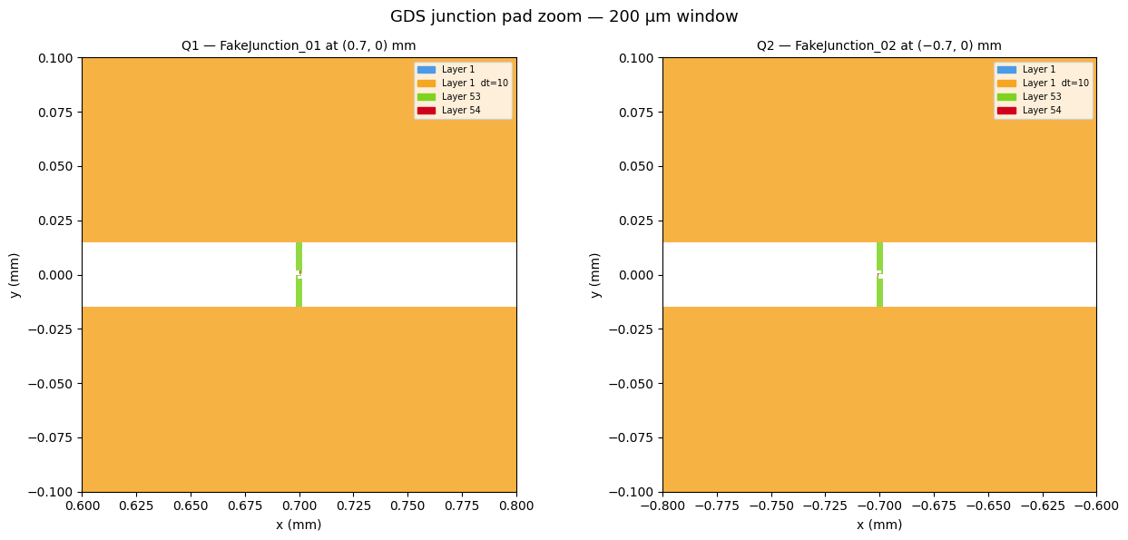
The plot_gds_zoom panels below colour each (layer, datatype) pair distinctly, making it easy to see where the junction sits relative to the qubit pads.
Zooming into junction pads in GDS
debug_summarize_gds_library gives a chip-level overview. To inspect individual junctions at fabrication scale, gds.plot_gds_zoom clips a small window out of the flattened GDS and renders it with matplotlib — no KLayout required.
It works by calling top.get_polygons(depth=None) to flatten the full cell hierarchy, filtering to a bounding box around your target, then drawing each polygon coloured by (layer, datatype).
Matplotlib backend note:
MetalGUIearlier in this notebook initialises PySide6, which can silently switch matplotlib to theQt6Aggbackend. With that backend active,plt.subplots()opens a Qt window instead of rendering inline. The%matplotlib inlinecell below resets to the staticAggbackend. This is expected any time Qt and matplotlib share a kernel; it is not a bug inplot_gds_zoom.
[16]:
# Reset to the static Agg backend so plots render inline.
# Needed because MetalGUI (used above) initialises PySide6 which can
# switch matplotlib to Qt6Agg. See the note in the markdown cell above.
%matplotlib inline
[ ]:
import matplotlib.pyplot as plt

# Zoom into each qubit — 200 µm window centred on the junction.
# Q1 sits at (0.70,  0) mm (orientation   0°) → junction cell rotated  90° → vertical
# Q2 sits at (−0.70, 0) mm (orientation 180°) → junction cell rotated −90° → vertical
fig, axes = plt.subplots(1, 2, figsize=(13, 6))
fig.suptitle("GDS junction pad zoom — 200 µm window", fontsize=13)

gds.plot_gds_zoom(
    lib,
    center_mm=(0.70, 0.0),
    span_mm=0.10,
    title="Q1 — FakeJunction_01 at (0.7, 0) mm",
    ax=axes[0],
)
gds.plot_gds_zoom(
    lib,
    center_mm=(-0.70, 0.0),
    span_mm=0.10,
    title="Q2 — FakeJunction_02 at (−0.7, 0) mm",
    ax=axes[1],
)

plt.tight_layout()
# plt.close(fig)
# fig
Viewing your GDS file
Once you have a .gds file, you’ll want to inspect it visually — zoom into junction pads, verify layer colours, check that routes don’t collide. Several free tools can do this on every platform.
KLayout (recommended)
KLayout is the industry-standard open-source GDS/OASIS viewer and editor. It handles multi-layer designs, has a Python scripting console, and runs on Windows, macOS, and Linux.
Install:
Platform |
Method |
|---|---|
macOS |
|
Windows |
Download the |
Linux |
|
Open your file:
# From the terminal — opens KLayout with the file loaded
klayout my_chip.gds
Or launch KLayout and use File → Open.
Key things to check:
Layer panel (right side) — toggle layers on/off to isolate metal, junctions, cheese holes
Ruler tool (
R) — measure distances in design unitsZoom to fit (
F) — see the full chip at onceZoom into junction pads — verify physical size matches your design (30 µm × 3 µm for the fake junctions here)
Quick in-notebook preview (no install needed)
You already have gdstk and the debug_summarize_gds_library tool. For a fast sanity check without leaving Jupyter:
import gdstk
lib = gdstk.read_gds("my_chip.gds")
gds.debug_summarize_gds_library(lib, show=True, scale=100, width=900)
This embeds an SVG overview directly in the cell output and saves with the notebook. Good for a quick geometry and layer check; use KLayout for detailed inspection.
Other free viewers
Tool |
Platform |
Notes |
|---|---|---|
Python (all platforms) |
Programmatic; |
|
Linux / macOS |
Full DRC + extraction; steeper learning curve |
|
Windows / Linux |
3D visualisation of GDS layers |
For more information, review the Introduction to Quantum Computing and Quantum Hardware lectures below
|
Lecture Video | Lecture Notes | Lab |
|
Lecture Video | Lecture Notes | Lab |
|
Lecture Video | Lecture Notes | Lab |
|
Lecture Video | Lecture Notes | Lab |
|
Lecture Video | Lecture Notes | Lab |
|
Lecture Video | Lecture Notes | Lab |